
Why is SiC Coated Wafer Carrier for Etching so Important in the Etching Process?
2025-07-11
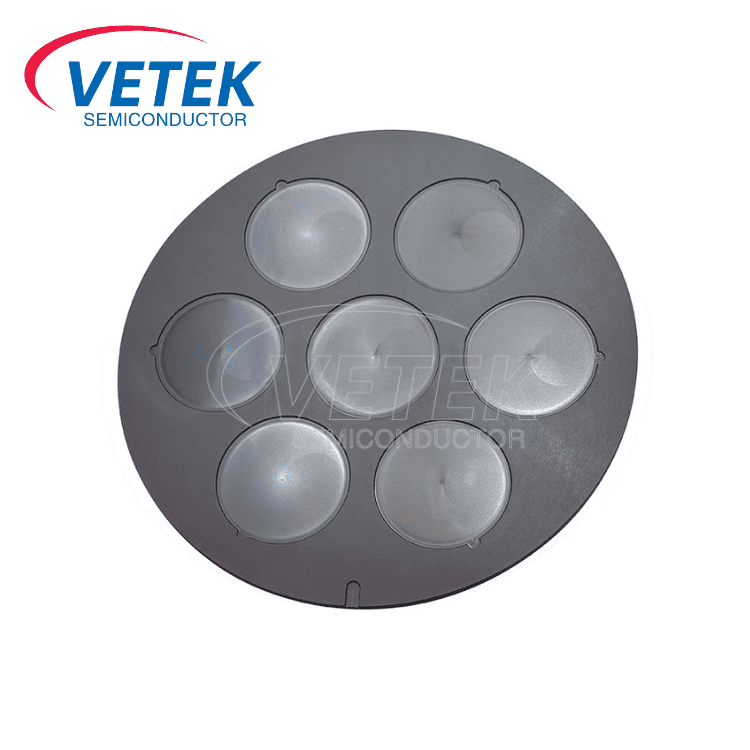
In the semiconductor manufacturing process, every step of wafer processing is related to the yield and consistency of the final product. Especially in high-temperature and highly corrosive environments such as etching, traditional quartz or graphite materials gradually show their limitations, while SiC Coated Wafer Carrier for Etching prepared by CVD provides a more reliable and advanced solution. The stability of SiC is particularly outstanding in high-temperature atmosphere or vacuum state, which not only improves the efficiency of continuous operation of equipment, but also significantly reduces the frequency and risk of carrier replacement. This material upgrade is not only a leap in performance, but also a new balance between process safety and equipment maintenance costs.
Why is SiC Coated Wafer Carrier an Advanced Choice in Extreme Environments?
The harshness of the etching process places extremely high tolerance requirements on the carrier, especially under frequent chemical cleaning and high-temperature cycles. SiC material naturally has strong acid and alkali resistance, and can resist erosion by highly corrosive media including hydrofluoric acid and nitric acid, making it one of the very few materials that can run stably in the front-end process. In contrast, traditional materials are prone to surface degradation due to microscopic erosion or stress cracks, which not only contaminates the wafer but also affects the repeatability of the process. Therefore, choosing our factory's SiC coated wafer carrier not only extends the product life, but also reduces the uncontrollable variables in the overall operation.
The role of thermal management in wafer processing is often underestimated, but in fact it is an important factor in determining the uniformity of thin film deposition and the consistency of etching rate. CVD SiC coating has extremely high thermal conductivity, which can quickly distribute heat evenly and effectively avoid local over-etching or film thickness deviation caused by temperature difference. At the same time, its excellent high-temperature mechanical strength allows the carrier to maintain structural integrity during repeated thermal cycles, reducing the incidence of problems such as fracture and delamination. These properties directly promote the improvement of SiC Coated Wafer Carrier for Etching yield, especially in the manufacture of power devices that are extremely sensitive to temperature control.
In ultra-clean semiconductor processes, any particles or metal ions may cause defects or even wafer scrapping. Using pressure-sintered silicon carbide (SSiC) as the substrate and applying a high-purity CVD SiC coating can significantly reduce surface roughness, reduce particle adhesion, and reduce the risk of contamination from the source. At the same time, the high purity (>99.9999%) and low defect density brought by the CVD process further ensure that the material will not release metal impurities in highly sensitive processes, greatly ensuring chip-level process safety, especially in the field of silicon carbide power devices and third-generation semiconductors.